How to design a PCB in KiCAD
Student Project House Zentrum, Clausiusstrasse, Kreis 6
About
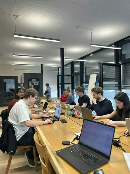
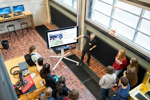
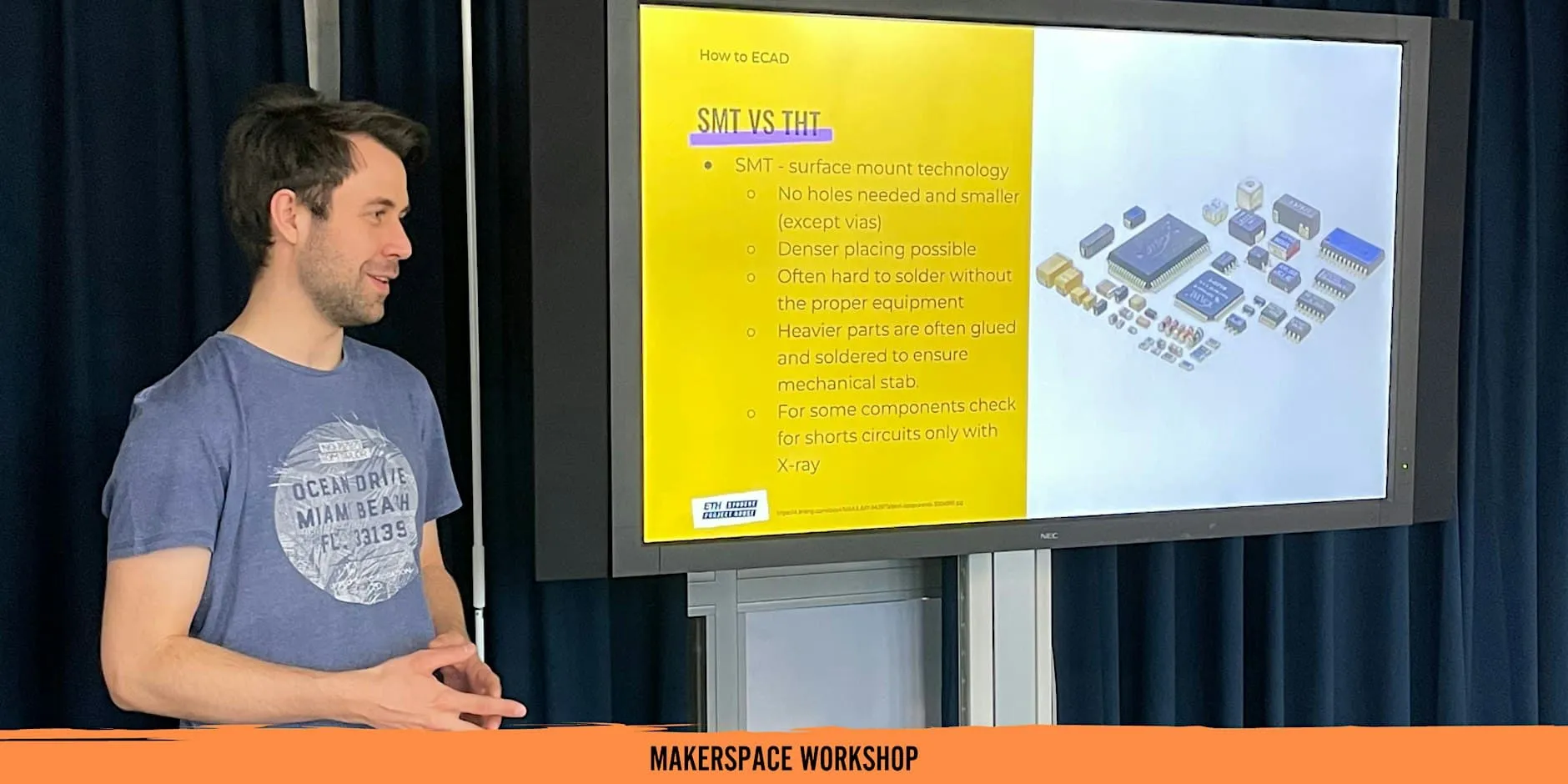
A workshop where participants learn step by step on their own laptop how to design their own printed circuit boards in KiCAD. It is run by the Student Project House at ETH Zürich, which also shares hands-on tips on creating PCBs in general. The workshop is for ETH students and limited to 12 participants so that everyone gets personalized support. Attendees should bring a laptop, charger and mouse, and install the free KiCAD software beforehand.
Written by a model, sources: sph.ethz.ch, eventbrite.ch
Venue
Student Project House Zentrum is in Zürich’s Kreis 6.
Clausiusstrasse
Student Project House Zentrum 24 more events